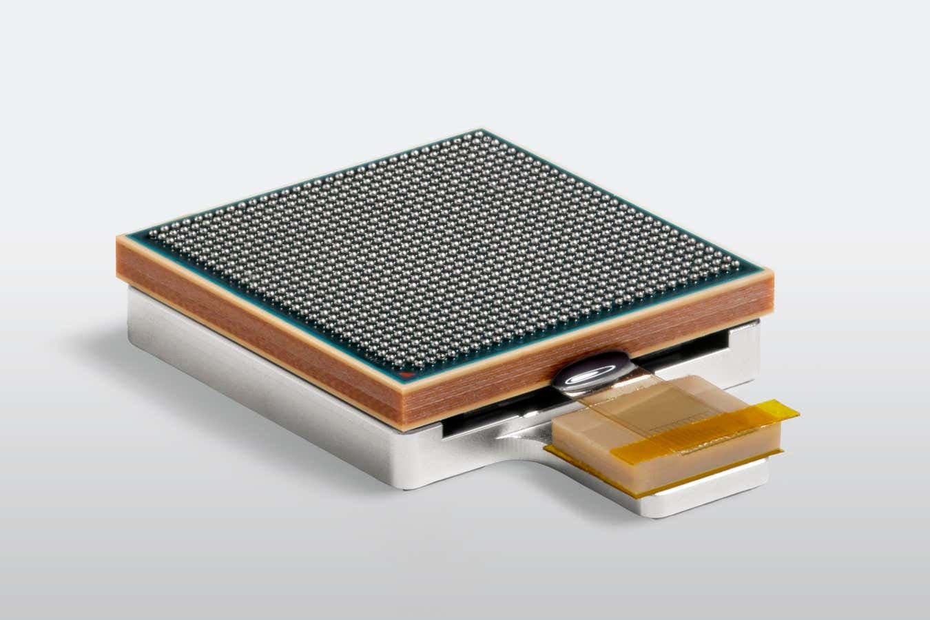
The prototype of an IBM optics module for connecting chips with fibre optics
Ryan Lavine for IBM
An optical fibre technology can help chips communicate with each other at the speed of light, enabling them to transmit 80 times as much information as they could using traditional electrical connections. That could significantly speed up the training times required for large artificial intelligence models – from months to weeks – while also reducing the energy and emissions costs for data centres.
Most advanced computer chips still communicate using electrical signals carried over copper wires. But as the tech industry races to train large AI models – a process that requires networks of AI superchips to transfer huge amounts of data – companies are eager to link chips using the light-speed communication of fibre optics.
This technology isn’t new: the internet already relies on undersea fibre-optic cables stretching thousands of kilometres between continents. In order to transmit data between fingernail-size chips, however, companies must connect as many hair-thin optical fibres as possible to the edge of each chip.
“As we all know, the best communication technology is fibre optics, and that’s why fibre optics is used everywhere else for long-distance communication,” said Mukesh Khare at IBM Research during a press briefing previewing the technology. “This co-packaged optics innovation is basically bringing the power of fibre optics on the chip itself.”
Khare and his colleagues have developed an optics module that would enable chipmakers to add six times as many optical fibres to the edge of a chip, compared to current technologies. The module uses a structure called an optical waveguide to connect as many as 51 optical fibres per millimetre. It also prevents light signals from one fibre from interfering with its neighbours.
“What IBM has really done here is use all of its materials and packaging technology – the history of leadership in that – to really break through how you do high-density fibre optics by using waveguides,” says Dan Hutcheson at TechInsights, a semiconductor tech research firm headquartered in Canada. “To me, that was the big breakthrough when I saw it.”
The resulting boost in communication between chips could enable AI developers to train a large language model within three weeks instead of three months. Switching from electrical wires to optical fibres for chip communication could also mean a fivefold reduction in the energy cost of training such AI models.
IBM has already put the optical module through stress tests that included high humidity and temperatures ranging from -40°C (-40°F) to 125°C (257°F). Hutcheson expects that major semiconductor manufacturing companies may be interested in licensing the technology.
“We’re really in the early days of all this, but it’s the hottest area in semiconductor technology right now in terms of high-performance computing and AI technology,” he says.
Topics:
- artificial intelligence/
- computing


Leave a Reply